Nanofader
Introduction
The Nanofader is an open-source active turntablist crossfader circuit which is designed to be as simple and cheap as possible. It uses standard jellybean CMOS chips rather than expensive specialised VCAs, and can easily be assembled on a prototype board if needed.
It was originally created to allow high-quality faders to be used with portable turntables such as the Numark PT-01, but the same circuit could be adapted to a number of different uses.
Description
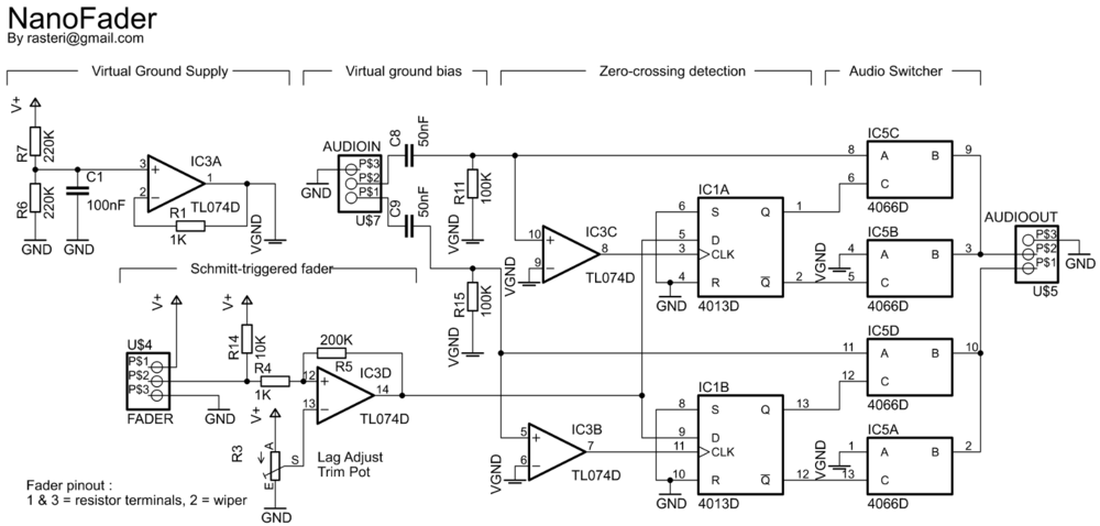
Schematic
Here is the nanofader circuit in its simplest form, with no signal buffering or power decoupling. This configuration requires only three ICs and can be built for less than £1 in parts (not including circuit board or connectors) :
Circuit Description
Full Article with awesome waveform diagrams and harmonic analysis : Decay
Muting an audio signal is not as simple as immediately returning the channel to zero. If the signal is at a voltage level of anything other than zero, the waveform will be chopped off, resulting in a nasty "click" or "pop" noise. Most performance mixers compensate for this by adding a volume decay, in which the signal is slowly muted over the course of 10-20 milliseconds. This has the advantage of sounding very smooth, but the decay time needs to be tuned very carefully to allow for properly-timed rhythmic scratches, and it generally requires a fairly complex and/or expensive VCA circuit. The nanofader works on a different principle - delayed zero-crossing detection.
The nanofader design works because the "pop" noise associated with immediately cutting a channel will not occur on a channel that is already at ground-level voltage. If we delay the muting signal until the next time the signal reaches ground-level, we can eliminate these nasty artifacts. All AC-coupled audio signals reach 0v regularly enough that delaying the cut until the next zero crossing will not noticeably affect the timing.
The design has four main subsections - the schmitt triggered fader, the zero crossing detection circuit, the delay circuit, and the audio switch.
- The schmitt-triggered fader circuit is essentially a comparator. When the fader voltage is below a certain threshold (set by the lag trim pot), the circuit outputs a logic 0, which is used to signal to the delay circuit that the channel should be muted.
- The zero crossing detection is another comparator with the threshold voltage set to 0v. This generates a digital logic signal that rises from low to high every time the audio signal crosses 0v. This is then used as the clock input for the delay circuit.
- The delay circuit takes the logic output from the schmitt trigger and delays it until the next time the clock input rises from low to high, i.e. when the audio signal crosses zero in the positive direction. This delayed signal is then passed to the audio switch.
- The audio switch simply switches the audio output between the input signal and ground level, depending on if the delayed signal is zero or one.
These subsections combine to ensure that the audio channel is only ever muted when the signal is at ground level, and as such is completely devoid of any unwanted switching noise.
Resources
Here is a zip file containing the latest schematic and board files in EAGLE format for the nanofader. This version has a proper mixer section with AUX in and output buffering/gain.
